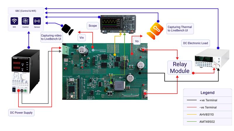
AHV85110 – Isolated GaN Gate Driver
The AHV85110 is a compact, isolated gate driver tailored for high-frequency GaN FET applications. It eliminates the need for bootstrap biasing through integrated isolated power delivery, making it ideal for compact, efficient high-voltage systems. Operating at 350 kHz, the device drives both high-side and low-side GaN switches in a half-bridge configuration. It supports a 48 V input and includes a 12 V on-board regulator for the gate drive supply. Its isolated design ensures robust high-speed switching and reduced EMI in high-performance power systems.
AMT49502 – Automotive MOSFET Gate Driver
The AMT49502 is an automotive-grade half-bridge MOSFET gate driver designed for 100 kHz switching operations. It integrates cross-conduction protection, under-voltage lockout, and thermal features, making it well-suited for traditional MOSFET-based designs. Operating from the same 48 V input, it includes a 5 V on-board logic supply and interfaces easily with external PWM signals from an MCU. It provides reliable, efficient switching for automotive and industrial converters.
Introduction to the Demo Board
The evaluation platform consists of two sections on a single PCB:
- GaN Section:
- 2 – AHV85110 gate drivers (high-side and low-side)
- Half-bridge GaN stage driven at 350 kHz
- MOSFET Section:
- An AMT49502 half-bridge driver
- Half-bridge MOSFET stage driven at 100 kHz
The board operates from a 48 V DC input, and includes on-board regulators to generate the 12 V and 5 V supplies required by the AHV85110 and AMT49502 respectively.
PWM control is supplied from an external MCU (e.g., Teensy 4.0), with manual or MCU-based enable/disable control options.
Gate Driver Evaluation Lab Overview
Measuring Efficiency Across Load Range
Users can perform an efficiency sweep by incrementing the load current in 0.5 A steps from 0.5 A to 3 A, helping visualize power delivery performance.
Analyzing Switching Node Waveform
At a fixed load of 3 A, users can capture and analyze real-time waveforms at the half-bridge switching nodes to observe rise/fall times, switching performance, overshoot behaviors and deadtime.
Performing Thermal Profiling
Thermal testing enables users to apply a constant load current (1–3 A) and monitor heat buildup via a thermal camera.