The semiconductor industry is evolving at a rapid pace, driven by advancements in artificial intelligence (AI), 5G, green technologies, and emerging markets like Automotive and IoT. In the last quarter of 2024, several trends have gained momentum, setting the stage for what is to come in 2025. This blog will delve into five of the most significant topics and provide a forward-looking perspective on their impact on the industry, particularly focusing on innovation and market transformation.
AI-Powered Semiconductor Design: The Role of Generative AI
Over the past few months, AI-powered semiconductor design, especially with generative AI tools, has gained remarkable attention. These AI tools help automate chip design, reducing time-to-market, lowering production costs, and enhancing performance through optimized architectures. This trend is driven by the necessity to develop advanced chips faster than ever due to the explosion of applications requiring high-performance computing, such as AI models and edge devices.
-Automation of Design Processes
AI tools like AlphaChip using Google’s DeepMind and Synopsys’ DSO.ai (Design Space Optimization AI) are now heavily integrated into chip design. These tools analyze past design successes and failures, automatically generating new chip architectures based on AI-optimized processes.
“AlphaChip has generated superhuman chip layouts used in every generation of Google’s TPU since its publication in 2020. These chips make it possible to massively scale-up AI models based on Google’s Transformer architecture.”
– Anna Goldie and Azalia Mirhoseini
-Energy Efficiency
AI-designed chips have indeed made significant strides in improving power efficiency, a critical factor in today’s IoT and mobile applications. In recent research, IBM highlighted advancements in this area, particularly in a paper where they demonstrated the potential of analog-AI systems. IBM’s approach combines time, area, and energy-efficient implementation of the on-chip auxiliary compute, showing how these designs can optimize not only individual chip performance but the entire system.
According to IBM, the breakthrough lies in the ability to sustain high energy efficiency and throughput during complex processes such as matrix–vector multiplication on analog-AI tiles. These advancements, when scaled to an entire system, provide excellent sustained efficiency across workloads. This is particularly impactful in AI-driven tasks, where power consumption is often a limiting factor. By leveraging these energy-efficient designs, industries dependent on AI, from autonomous systems to mobile devices, will be able to push performance limits without compromising on sustainability.
“IBM showed it’s possible to build analog AI chips that can handle natural-language AI tasks with an estimated 14 times more energy efficiency.”- IBM
Future Insight for 2025
In 2025, we anticipate further advancements in generative AI, enabling the development of self-optimizing chips. These chips could autonomously adapt their performance based on the workload, reducing power consumption and heat dissipation. AI-powered design will likely dominate semiconductor manufacturing processes, cutting down both the human labor and time required to develop cutting-edge chips.
The Shift Towards 3D Chip Architectures
One of the hottest topics in semiconductor manufacturing is the move toward 3D chip architectures. Instead of relying on traditional 2D planar designs, manufacturers are now stacking chips vertically, offering improved performance, reduced latency, and lower power consumption. This shift is driven by the increasing demand for more processing power in a smaller footprint, especially in data centers, smartphones, and AI accelerators.
-TSMC and Intel’s Focus on 3D Designs
Foundries like TSMC and Intel are leading the charge in 3D stacking technology, with Intel’s Foveros and TSMC’s Chip-on-Wafer-on-Substrate (CoWoS) becoming industry standards.

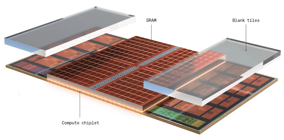
AMD’s 3D V-Cache tech attaches a 64-megabyte SRAM cache [red] and two blank structural chiplets to the Zen 3 compute chiplet made by TSMC’s wafer-on-wafer, where an entire wafer of one type is bonded to an entire wafer of the other, then diced up into chips.
“Despite tripling the L3 [cache] size, 3D V-Cache only added four [clock] cycles of latency—something that could only be achieved through 3D stacking,”
-Heterogeneous Integration
Combining different types of semiconductors, such as memory and logic, in a 3D stack is becoming more common, allowing for specialized chips tailored to specific applications like machine learning or high-performance computing. Like the monolithic three-dimensional integration (M3D) of hybrid memory architecture based on resistive random-access memory (RRAM), named M3D-LIME.

Fig: Architecture of the M3D-LIME chip
Future Insight for 2025
By 2025, 3D chip architectures will become the standard for high-performance computing applications, especially in AI and quantum computing. These chips will be crucial in reducing energy consumption in data centers, which have become massive energy consumers globally. Expect to see major players like NVIDIA and AMD adopt these architectures for their next generation of GPUs.
Chip Supply Chain Resilience and Localization Efforts
The chip shortage of the past few years highlighted the vulnerabilities in the global supply chain. Over the last quarter, there has been a surge in efforts to build more resilient and localized supply chains for semiconductor manufacturing. Countries like the United States and European Union are investing billions into onshore chip manufacturing, aiming to reduce dependency on a few key players like Taiwan and South Korea.
-CHIPS Act in the U.S.
The U.S. government passed the CHIPS and Science Act to incentivize domestic semiconductor manufacturing. Companies like Intel and Micron have announced new fabs in the U.S.
-EU’s Semiconductor Push
Europe is also making strides with its own semiconductor initiatives, aiming to double its share of global chip production by 2030.
Future Insight for 2025
By 2025, expect a more diverse and localized semiconductor supply chain, which will mitigate the risks of future chip shortages. While Taiwan and South Korea will continue to play dominant roles, the U.S. and EU will emerge as critical players in the global semiconductor landscape, promoting more geopolitical stability in the supply chain.
Green Semiconductors and Sustainability Initiatives
Sustainability in semiconductor manufacturing has become a pressing concern, with companies and governments pushing for more **eco-friendly production methods**. The semiconductor industry has a large environmental footprint, from water and energy usage to chemical waste. Over the past quarter, there has been a surge in innovations aimed at reducing this impact.
-Energy-Efficient Chip Designs
Companies are developing chips that use less power and produce less heat, such as GaN (Gallium Nitride) and SiC (Silicon Carbide) semiconductors, which are known for their efficiency in high-power applications.
-Water Conservation Initiatives
The semiconductor industry is notorious for its massive water consumption, especially during the chip fabrication process. As environmental concerns rise, semiconductor fabs are increasingly adopting water recycling technologies to address this issue. These technologies are designed to reduce water usage and lower the industry’s environmental footprint, aligning with broader sustainability goals.
“TSMC chip fabs in Taiwan achieve a nearly 90% water recycling rate”- A TSMC spokesperson to Business Insider
To receive funding from the new CHIPS and Science Act, fabs in USA could face extensive federal reviews under the 1970 National Environmental Policy Act, which requires federal agencies to assess each project’s potential environmental impact.
-Cloud-Based IC Evaluation
TenXer Labs is at the forefront of driving digitalization and sustainability in the semiconductor space with its cloud-based IC evaluation platform LiveBench. This platform allows companies to remotely evaluate and test integrated circuits (ICs) without the need for physical prototypes. With just one evaluation kit (EVK), engineers can conduct 100+ evaluations globally. This significantly reduces the carbon footprint by cutting down on shipping, material waste, and travel, while accelerating the testing process. By digitizing the IC evaluation process, TenXer Labs is helping companies meet their sustainability goals while maintaining the pace of innovation.
Future Insight for 2025
In 2025, green semiconductor manufacturing will not just be an industry buzzword but a competitive differentiator. Companies that lead in energy efficiency, carbon neutrality, and eco-friendly production will have a significant market advantage. As seen with Tenxer Labs’ cloud-based IC evaluation, the push for digitalization will further reduce waste and resource consumption in the industry, enabling more sustainable business models. Regulations on sustainability in manufacturing will likely tighten, and companies will need to innovate rapidly to comply.
Semiconductors for the Automotive Industry: The Rise of EVs and Autonomous Driving
The automotive industry has become one of the largest consumers of semiconductors, driven by the shift toward electric vehicles (EVs) and autonomous driving technologies. In the last quarter, advancements in chips specifically designed for these applications have surged, especially in the areas of power management, sensor fusion, and AI processing.
-EV Power Management
Chips that manage power in EVs, such as SiC-based inverters, are improving the efficiency and range of electric vehicles. Companies like Infineon and STMicroelectronics are leading this space.
-AI for Autonomous Driving
AI chips designed for real-time decision-making are becoming more powerful and energy-efficient. NVIDIA’s Drive Orin platform, for instance, has become the go-to choice for many automakers in autonomous driving.
“Orin achieves 200 TOPS — nearly 7x the performance of the previous generation SoC Xaiver — and is designed to handle the large number of applications and deep neural networks that run simultaneously in autonomous vehicles and robots, while achieving systematic safety standards such as ISO 26262 ASIL-D.”- NVIDIA
Future Insight for 2025
By 2025, semiconductors will become the backbone of the Automotive industry, with EVs becoming mainstream in many parts of the world. Autonomous driving technologies will also mature, fueled by advancements in Edge AI processing and sensor technologies. Automotive-grade chips will see exponential growth, and innovations in chip reliability for extreme conditions (temperature, vibration) will be critical for success in this market.
A Look Ahead to 2025
The semiconductor industry is entering a transformative era. With AI-powered design, 3D chip architectures, localization of supply chains, green semiconductor initiatives, and the expansion of chips in the automotive industry, the sector is poised for tremendous growth and innovation in 2025. Companies that prioritize sustainability, resilience, and AI-driven efficiencies will lead the way, reshaping not only the semiconductor landscape but also the broader technology market.
At the forefront of this transformation is TenXer Labs, driving the push toward digitalization and sustainability in IC evaluation. As cloud-based solutions continue to replace traditional, resource-intensive evaluation methods, Tenxer Labs is helping companies reduce their carbon footprint while increasing operational efficiency. Through remote evaluation with just one EVK for 100+ evaluations, businesses can embrace more sustainable practices and contribute to a greener future.
As we approach 2025, staying at the cutting edge of these trends will be essential for companies and industry professionals alike. TenXer Labs believes that by embracing digitalization, cloud solutions, and sustainable innovation, the semiconductor industry can not only meet growing technological demands but also create a positive impact on the environment. Semiconductor technology will continue to drive the global economy, and those who adapt quickly to these innovations will thrive in the competitive landscape ahead.


