Provide Feedback

The Future of Electronics Design and Development: Can We Cut the Carbon Footprint?

The Hidden Environmental Cost of Electronics Design

Electronics systems power everything from smart appliances to industrial automation. However, the development process behind these systems has an overlooked environmental impact—one that contributes to carbon emissions, electronic waste (e-waste), and energy consumption. 

Traditional design and development relies on physical Evaluation Kits (EVKs), local lab setups, and resource-heavy workflows that generate a significant carbon footprint. As companies work toward sustainability goals, it’s time to rethink how embedded engineering can become more eco-friendly. 


In this article, we’ll break down the environmental impact of traditional development and explore ways to reduce CO₂ emissions while maintaining efficiency and innovation. 

How Traditional Development Impacts the Environment

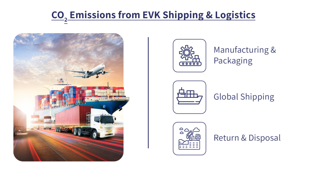
  1. CO₂ Emissions from EVK Shipping & Logistics

Evaluation Kits (EVKs) are essential for engineers testing microcontrollers (MCUs), microprocessors (MPUs), and other embedded components. However, these kits must be manufactured, packaged, and shipped worldwide, adding CO₂ emissions at every stage: 


Manufacturing & PackagingProducing an EVK involves PCB fabrication, component assembly, plastic enclosures, and packaging materials. Each step consumes resources and generates carbon emissions. 

Global ShippingEVKs often travel thousands of kilometers via air, sea, or road freight. A single shipment from Asia to Europe or North America can emit over 100 kg of CO₂. 

Return & DisposalOnce testing is complete, unused or obsolete EVKs may be discarded or stored indefinitely, contributing to e-waste accumulation. 

Annual Carbon Footprint
A company evaluating 20 EVKs per year could generate over 2,000 kg of CO₂ just from shipping-related emissions. 


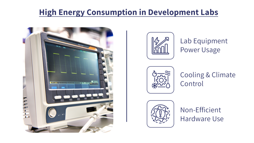
  1. High Energy Consumption in Development Labs

Embedded development requires dedicated workstations, test setups, and continuous power usage. Unlike cloud computing, which optimizes energy usage at scale, on-premise development labs consume excessive power due to: 


Lab Equipment Power UsageTest setups, oscilloscopes, power supplies, and workstations run 24/7, leading to high electricity consumption. 

Cooling & Climate ControlMany labs require air conditioning or specialized cooling to maintain optimal conditions, increasing their energy footprint. 

Non-Efficient Hardware UseEngineers often need multiple EVKs and test rigs for different projects, leading to redundancy and waste. 

Annual Carbon Footprint 
A single development lab can consume as much electricity as 4–5 homes, translating to over 5,000 kg of CO₂ emissions per year. 


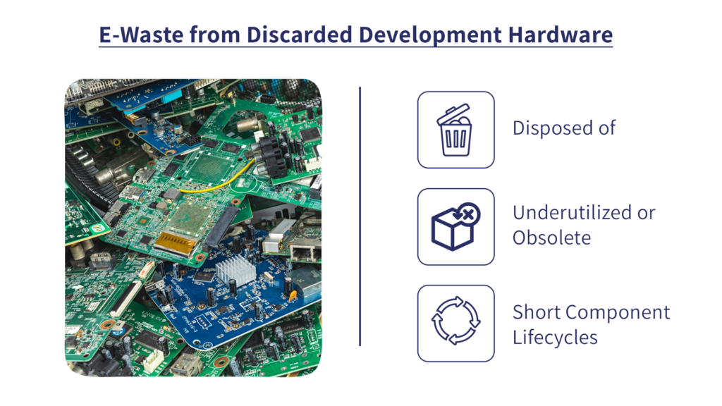
  1. E-Waste from Discarded Development Hardware

E-waste is one of the fastest-growing environmental challenges, and hardware-driven embedded development contributes to this problem. Once projects end or technology evolves, EVKs and test hardware are often: 


Disposed ofMany development kits end up in landfills, where electronic components leach hazardous materials into the environment. 

Underutilized or ObsoleteEngineers frequently upgrade to newer platforms, making older evaluation boards unusable for future projects. 

Short Component LifecyclesMany semiconductor manufacturers discontinue support for older EVKs within 3–5 years, forcing companies to purchase new kits.

Global E-Waste Impact

The world generates 50 million tons of e-waste annually and the electronics industry—including embedded systems—is a key contributor.

How Can We Reduce the Carbon Footprint of Electronics Design and Development?

With increasing focus on sustainability, engineering teams and semiconductor manufacturers must adopt greener alternatives. 


  • Reduce Hardware DependencyMove towards cloud-based evaluation environments to minimize reliance on physical EVKs. 
  • Optimize Resource Sharing Instead of dedicated hardware per engineer, enable remote access to evaluation hardware, reducing redundant equipment. 
  • Use Cloud-Based EvaluationSolutions like LiveBench provide remote evaluation platforms, eliminating the need for shipping and maintaining local test setups. 
  • Adopt Circular Economy PracticesExtend the lifespan of EVKs, promote recycling programs, and encourage manufacturers to develop more sustainable hardware. 

Join the Sustainability Pledge

Be part of a movement redefining electronics design for a greener future.

Introducing the TenXer Carbon Footprint Calculator

At Embedded World 2025, check-out our CO2 Calculator that can measure and compare the environmental impact of traditional hardware-based versus cloud-based evaluation.
Know More

Are You Ready to Lead the Change?

The electronics industry has long optimized for performance and efficiency—now it’s time to optimize for sustainability. Be among the first to experience this exclusive launch at Embedded World 2025 and take a step toward smarter, greener electronics ecosystem.  

Meet us at embedded World Germany

Table of Contents

Share the Post:
  • Priyanka C

    As the Director of Marketing at TenXer Labs, Priyanka spearheads strategic initiatives to position the company as a leader in the semiconductor industry. Leveraging her extensive experience over 10 years, she crafts compelling narratives that highlight TenXer Labs' solutions, fostering brand awareness and driving business growth.

Related Reads
Cloud vs. On-Premise Labs – Energy Efficiency & CO₂ Savings
Feb 21, 2025
Read More
Real-Time Insights with the World’s Smartest AI Enabled Trail Camera
Feb 7, 2025
Read More
Evaluating MCU Performance with Network-on-Chip (NoC) Connectivity with Remote Labs
Jan 23, 2025
Read More

Was the content on this page helpful?