
Introduction to Boost DC-DC Converter Design
A boost converter, often referred to as a step-up converter, is a widely used power electronics circuit designed to increase the input voltage to a higher output voltage while maintaining efficient energy transfer. This circuit topology plays a crucial role in modern power systems, especially in applications where the supply voltage is lower than the desired output voltage, such as in solar panels, batteries, or low-voltage power sources.
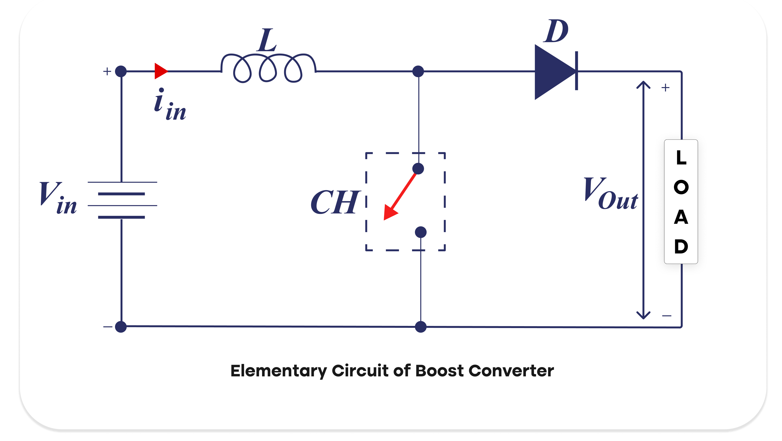
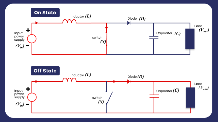
The boost converter consists of essential components like an inductor, switch (S), diode (D), and an output capacitor, which work in tandem to regulate the output current and maintain a stable output voltage. The basic principle revolves around storing energy in the inductor’s magnetic field during the on state of the switch and releasing it during the off state, where the diode prevents current flow in the reverse direction. This enables efficient step-up conversion for a range of dc voltage applications.
The design of a boost converter involves several key parameters, including the switching frequency, inductor value, and duty cycle, which determine the inductor current and the energy stored. The MOSFET switches and Schottky diode are critical to achieving high efficiency and minimizing voltage drop.
Additionally, the output capacitor smooths the voltage ripple to ensure a steady output current. Energy storage elements like the inductor and capacitor work under varying load conditions, including light loads, to maintain the desired performance. Equations show how parameters like voltage across the components and the current paths during operation define the converter’s behavior. This versatile circuit is fundamental to power supply systems, offering high efficiency and reliable operation for applications requiring output voltage greater than the input source voltage.
Basics of Boost Converter
A boost converter is a type of DC-DC converter that steps up the input voltage to a higher output voltage, making it crucial for applications like batteries, solar panels, and other low-voltage sources. Its operation is based on the basic principle of storing energy in the inductor’s magnetic field during the on state of a switch and releasing it to the load during the off state, where the diode D becomes forward biased, allowing current flow to the load, while remaining reverse biased during the on state to prevent current flow back to the input.
Essential passive components like the inductor, capacitor, and diode, combined with at least two semiconductors, manage the energy transfer. The inductor releases stored energy during the switch’s off state, while the output capacitor reduces voltage ripple to stabilize the output voltage. Factors such as switching waveform, switching frequency, and duty cycle affect the inductor current and overall performance. A Schottky diode is often used for its low voltage drop, minimizing losses and enhancing efficiency. With this circuit topology, the energy storage element ensures consistent power supply to the load, even under light loads, making boost converters essential for high-efficiency power systems.
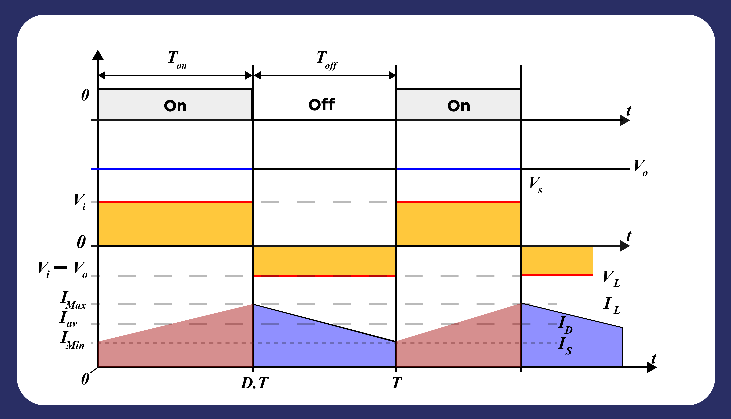
1.1. Operating Principle
A boost converter comprises an inductor, a switch (typically a transistor), a diode, and an output capacitor. The converter operates by storing energy in the inductor when the switch is closed and transferring this energy to the load when the switch is open. During operation:
Switch ON: The inductor stores energy as current flows through it, and the diode blocks the output.
Switch OFF: The inductor releases the stored energy to the load via the diode, raising the output voltage.
1.2. Key Components
- Inductor: Stores and releases energy to regulate the voltage.
- Switch: Generally a MOSFET or IGBT, controls the on-off cycles.
- Diode: Provides a path for current when the switch is off.
- Capacitor: Smooths the output voltage, reducing ripples.
1.3. Boost Converter Equation
The basic voltage relationship for a boost converter is:
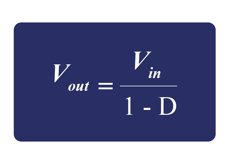
Where:
- Vout is the output voltage
- Vin the input voltage
- D is the duty cycle, defined as the fraction of time the switch is ON
As D increases, the output voltage becomes higher than the input voltage.
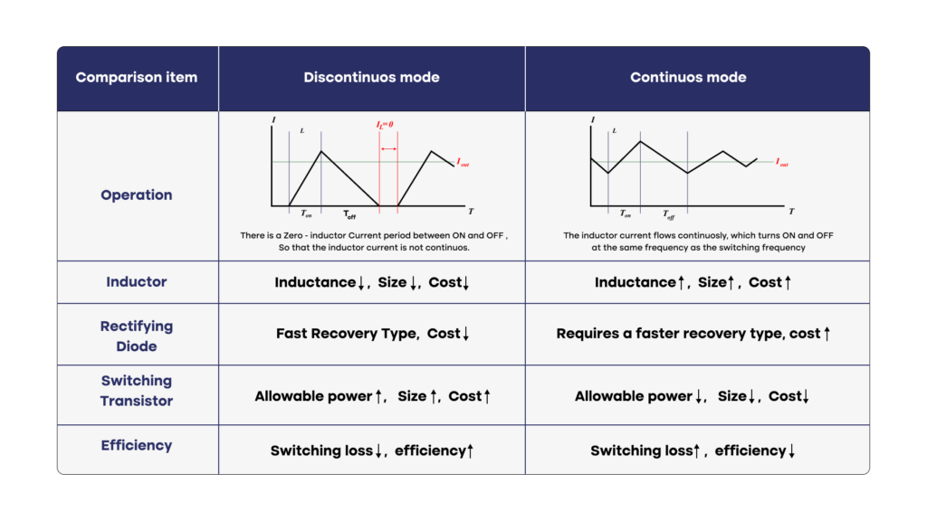
Continuous Conduction Mode (CCM)
Continuous Conduction Mode (CCM) in a boost DC-DC converter occurs when the inductor current never falls to zero during the switching cycle. This mode is characterized by a continuous flow of current through the inductor, even when the switch is turned off. In CCM, energy is stored in the inductor during the ON state and released to the load in the OFF state. CCM operation typically leads to higher efficiency at moderate to high loads, but requires careful design to ensure stability and proper component sizing, as it affects the converter’s transfer function and dynamic response.
2.1. Operation in CCM
In Continuous Conduction Mode (CCM), the inductor current never falls to zero during the switching cycle. This mode is typically desired for high-power applications where a smooth and continuous current is beneficial. The inductor stores energy when the switch is ON and releases it when the switch is OFF, ensuring that the current through the inductor is always positive.
2.2. CCM Waveforms
- Inductor Current: The current rises during the ON period and falls during the OFF period, but never reaches zero.
- Capacitor Voltage: The voltage across the capacitor is relatively stable with low ripple.
2.3. CCM Design Considerations
- Inductor Size: A large inductor is required to ensure that the inductor current does not drop to zero, leading to continuous conduction.
- Duty Cycle: The duty cycle affects the output voltage. For higher voltages, the duty cycle must approach but not exceed 1.
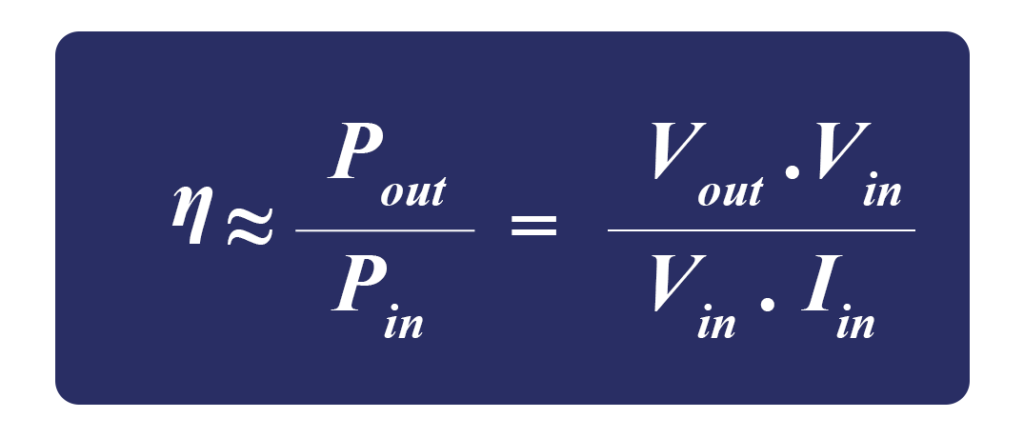
2.4. Efficiency in CCM
Efficiency is generally higher in CCM compared to DCM because the losses associated with switching and inductor current are minimized. The efficiency of a boost converter in CCM can be approximated by:
Discontinuous Conduction Mode (DCM)
Discontinuous Conduction Mode (DCM) in a boost DC-DC converter occurs when the inductor current falls to zero during each switching cycle, resulting in intervals where the inductor is not conducting. This mode typically happens at low load conditions or low input voltage, where the energy stored in the inductor is insufficient to sustain continuous current. In DCM, the converter operates in a non-linear fashion, with a different transfer function compared to Continuous Conduction Mode (CCM). DCM can lead to reduced efficiency but simplifies control in certain low-power applications due to its inherent switching characteristics.
3.1. Operation in DCM
In Discontinuous Conduction Mode (DCM), the inductor current falls to zero during part of the switching cycle. This mode typically occurs at light loads, where the energy transferred during each switching cycle is smaller.
3.2. DCM Waveforms
- Inductor Current: The current rises during the ON period, falls to zero during the OFF period, and remains at zero for a portion of the switching cycle.
- Capacitor Voltage: The voltage across the capacitor may have more ripple due to the intermittent nature of the current.
3.3. DCM Design Considerations
- Inductor Size: A smaller inductor can be used in DCM, reducing the overall converter size and cost. However, this comes at the expense of higher current ripple.
- Control Complexity: DCM introduces more complexity into the control design due to the non-linear behavior of the inductor current.
3.4. Efficiency in DCM
DCM can be less efficient than CCM at light loads due to increased switching losses and higher current ripple. However, for certain applications, such as low-power systems, DCM is preferred because it reduces the size and cost of the inductor.
Transfer Function of Boost Converter
The transfer function of a boost converter describes the relationship between the input voltage, output voltage, and control input (typically duty cycle) in both continuous conduction mode (CCM) and discontinuous conduction mode (DCM). In CCM, the transfer function can be derived by modeling the converter’s small-signal behavior using state-space averaging techniques. It shows that the output voltage is inversely proportional to the duty cycle, meaning that as the duty cycle increases, the output voltage rises. The system is non-linear, but linearization around an operating point helps analyze stability and dynamic response. In DCM, the transfer function becomes more complex due to the intermittent current flow, and this affects the converter’s efficiency and transient behavior.
4.1. Small-Signal Modeling
To design a stable control loop, it is crucial to understand the small-signal behavior of the boost converter. A small-signal model captures how the output voltage responds to small perturbations in the input voltage, duty cycle, or load.
For the boost converter, the duty cycle to output voltage transfer function in CCM can be expressed as:
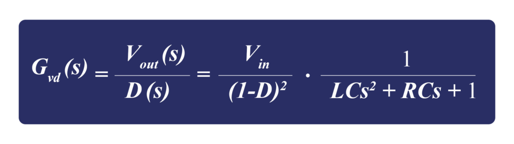
Where:
- L is the inductance
- C is the capacitance
- R is the load resistance
- S is the Laplace variable
4.2. Poles and Zeros
The transfer function typically has two poles, resulting in a second-order response. The location of the poles and zeros impacts the stability and dynamic response of the converter.
- Poles: Determined by the inductor and capacitor values, the poles dictate the natural frequency and damping of the system.
- Zeros: The right half-plane zero is a key characteristic of boost converters, which can complicate control design.
4.3. Control Design
A typical approach to control boost converters is using a Proportional-Integral (PI) or Proportional-Integral-Derivative (PID) controller. The control loop adjusts the duty cycle to regulate the output voltage in response to changes in the input or load.
Stability Analysis
Stability analysis of a boost converter is critical to ensure reliable and efficient operation. It involves examining the system’s dynamic behavior, particularly how it responds to disturbances or changes in load or input voltage. This is done by analyzing the converter’s transfer functions and ensuring that the feedback loop is stable under continuous conduction mode (CCM) and discontinuous conduction mode (DCM). Techniques such as Bode plot analysis are commonly used to assess the phase margin and gain margin, ensuring that the system can return to its equilibrium state without oscillations or instability when subjected to disturbances. Proper compensation design in the feedback loop is essential for maintaining stable operation.
5.1. Bode Plot
A Bode plot is an essential tool in power converter design. It provides a graphical representation of the gain and phase of the system across different frequencies, helping to assess stability. For a boost converter, the Bode plot reveals the system’s gain margin and phase margin, which indicate how far the system is from instability.
5.2. Phase Margin
The phase margin is the difference between the phase of the system and -180° when the open-loop gain crosses 0 dB. A phase margin of 45° to 60° is typically considered stable for power converters.
5.3. Gain Margin
The gain margin is the amount of gain that can be added to the system before it becomes unstable. A higher gain margin ensures that the converter remains stable under varying load and input conditions.
Design Procedure for Boost Converter
Begin by defining the required specifications, including input voltage, output voltage, load current, switching frequency, and efficiency targets. These parameters form the basis for component selection and design.
6.1. Component Selection
- Inductor: The inductor value is chosen based on the desired current ripple and operating mode (CCM or DCM).
For CCM operation:
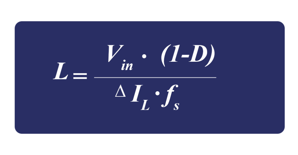
Where ΔIL is the desired inductor current ripple, and fs is the switching frequency.
Capacitor: The output capacitor is selected to ensure low output voltage ripple.
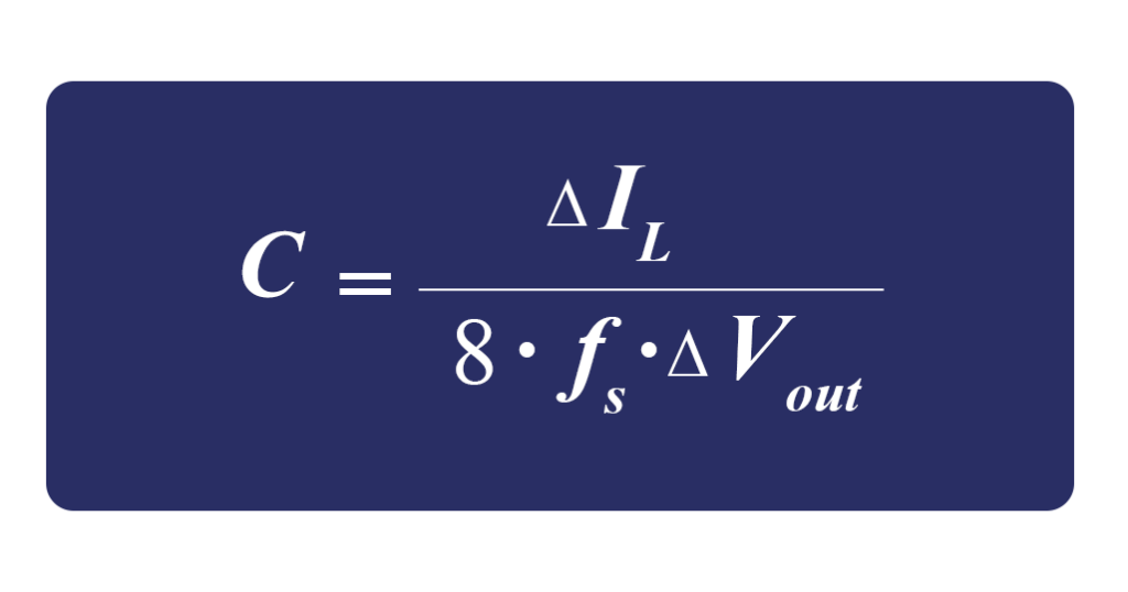
Where ΔVout is the allowable output voltage ripple.
- Switch: The switch must be rated for the peak current and voltage stress. MOSFETs are often chosen for their low ON-resistance and fast switching capabilities.
- Diode: The diode must handle the output current and withstand the reverse voltage when the switch is ON.
6.2. Thermal Design
Ensure that the components selected can dissipate the heat generated during operation. Use heat sinks or proper PCB layout techniques to manage thermal performance, especially at high power levels.
6.3. Control Loop Design
Implement a control loop using either analog or digital methods. The loop compensator (e.g., PI or PID controller) must be designed to achieve the desired dynamic response while maintaining stability.
6.4. Simulation and Prototyping
Before building the physical converter, use simulation tools (e.g., MATLAB, LTSpice) to validate the design. Simulations provide insight into transient response, stability, and efficiency. Once the design is verified, proceed with prototyping and testing.
Conclusion
Boost DC-DC converters are essential in modern power electronics systems due to their ability to efficiently step up voltage levels while maintaining high efficiency. Understanding their operation in CCM and DCM, analyzing transfer functions, and ensuring stability through proper control design are critical steps in developing a reliable
Dive deep into the world of DC/DC converters with our extensive lab selection. Evaluate transient response, load regulation, and efficiency across a vast array of topologies and leading manufacturers.