Enable Your Customers to Evaluate Instantly

Cloud Solutions for Faster Adoption of your ICs and Electronic Sub-systems with 24x7 Remote Labs

5x

Lower Customer Acquisition Costs

50%

Faster Sales Cycle

banner img
Instant Evaluation from Your Browser

Smarter Approach to IC Evaluation

Image

Accelerating Adoption through Innovation

Democratizing access to all semiconductor chips

TenXer Labs is a group of passionate engineers and technology geeks united by a shared goal – breaking barriers with innovation.

Featured Labs

Ultra-thin High Efficiency 72W DC-DC Converter Module – MYC0409-NA-EVM

Ultra-thin High Efficiency 72W DC-DC Converter Module – MYC0409-NA-EVM

This EVM features the Ultra-thin High Efficiency 72W DC-DC Converter Module – MYC0409-NA standalone charge pump module configured for operation with 20–60V input voltage range. The output voltage is fixed by divide-by-4 conversion ratio from input voltage. A synchroniser with an external clock can be set with a jumper. The full output current rating of the device can be supplied by the EVM. Input and output capacitors are mounted on the board to accommodate the entire range of input and output voltages. Monitoring test points are provided to allow measurement of voltage, efficiency, power dissipation and load regulation.  Control jumpers and component footprints are provided for use of the ENABLE, PGOOD, and CLK features of the module. The EVM uses a recommended PCB layout that minimizes output ripple and noise.

Launch Lab
Synchronous DC-DC Boost Converter - EV3428A-L-00A

Low IQ Boost Regulator Evaluation Board – LT8365

Low IQ Boost Regulator Evaluation Board – LT®8365 is a boost converter. It operates with a switching frequency of 400kHz and is designed to convert a 9V to 30V source to 250V, with 10mA output current. The demo board contains an optional third charge pump stage for applications requiring higher output voltages. If needed, remove R14 and install optional components. Output voltage sensing connections remain the same. The LT8365 can be used for different topologies with input voltages up to 60V. However, component selection in this demo circuit restricts the input voltage to 30V.

Launch Lab
Synchronous DC-DC Boost Converter - EV3428A-L-00A

DC-DC Synchronous Boost Converter – EV3428A-L-00A

The DC-DC Synchronous Boost Converter – EV3428A-L-00A Evaluation Board is designed to demonstrate the performance of MPS’ MP3428A, which has excellent protection and can provide load with 12V/2A power from typical 3.3V input. The MP3428A is a 600 kHz fixed frequency, high efficiency, wide input range, current mode boost converter with optional internal or external current sensing configuration for high integration and high power application. It features internally a 10mΩ, 24V power switch and a synchronous gate driver for high conversion efficiency. The MP3428A is available in a low profile 22-pin 3mmx4mm QFN package.

Launch Lab

DC-DC Low IQ Boost Converter

The LT8364 from Analog Devices is a current mode DC/DC converter with a 60 V, 4 A switch operating from a 2.8 V to 60 V input. It is capable of boost, SEPIC or inverting configurations. Burst Mode operation consumes as low as 9µA quiescent current to maintain high efficiency at very low output currents.

Launch Lab

DC-DC μModule Buck Regulator

The LTM4653 from Analog Devices is an ultralow noise 58 V, 4 A DC/DC step-down μModule regulator designed to meet the radiated emissions requirements of EN55022. Conducted emission requirements can be met by adding standard filter components. 

It operates over an input voltage range of 3.1 V to 58 V and supports an output voltage range of 0.5 V to 94% of VIN, and a switching frequency range of 250kHz to 3MHz (400kHz default).

Launch Lab

Synchronous DC-DC Buck Regulator

The MIC28517 from Microchip is a wide input range (4.5 V to 70 V) integrated FET, 8A switching regulator. Leveraging the latest enhanced high voltage COT controllers co-packaged with a pair of low FOM power trench N-Channel FETs with improved avalanche rating, the MIC28517 ensures efficient power management. 

The output voltage is adjustable down to 0.6 V with +/- 1% accuracy, making it suitable for various applications requiring precise voltage regulation.

Launch Lab
iW248 single chip
Renesas

Energy-Efficient Single-Burner Induction Cooktop using iW248 single chip ASSP

The 2100 W single plate induction cooktop design, using iW248 single chip ASSP offers high efficiency and high reliability performance.

The design gives the flexibility to adjust the power in +/-10 W steps, which allows the users to cook at a simmering condition. The RL78/G15 based HMI card offers low pin count, multiple matrix switch, LED Indication, and 7-Segment display. Over-temperature detection using three NTCs are provided in the ASSP.

Launch Lab
RZV2M Vision AI Platform Reference Design
Renesas

RZ/V2M: Vision AI Platform Reference Design

The RZ/V2M evaluation board is capable of easily implementing software development such as camera sensor input image processing, low power consumption AI inference, and video streaming.

The system integrates the Sony IMX568 camera sensor, which features a global shutter image sensor.

The RZ/V2M utilizes the DRP-AI implementation of the compact YOLOv2 application, integrated with ISP support package, specifically tailored for the IMX568 camera.

The LiveBench implementation of the Vision AI on RZ/V2M with IMX568, Global Shutter Image Sensor allows customers to evaluate the RZ/V2M capability to process the images captured from the Sony IMX568 with following setup:

  • By employing an external image rotation system.
  • The setup validates the built-in global shutter capabilities of the Sony IMX568 camera sensor, with assistance from the RZ/V2M platform.
Launch Lab
RX231 DSP
Renesas

RX Family DSP Solution

The RX 231 (DSP processor family) performs analog signal input, IIR filter, FFT, and HMI processing with a single microcontroller. 

The LiveBench implementation of the RX231 allows the customers to accurately analyze signal frequency and amplitude under various filtering conditions. 

This test setup will allow customers to do the following: 

  • Calculate FFT from live signal and measure accuracy of signal;
  • Apply filtering and signal conditioning. 
Launch Lab
Buck boost controller
Renesas

High Voltage Synchronous Buck-Boost Controller

The ISL81801EVAL1Z evaluation board includes the ISL81801, an 80V bidirectional synchronous buck-boost controller with a constant voltage/current output. A customizable switching frequency ranging from 100kHz to 600kHz aids in optimizing inductor size, while the robust gate driver allows for high power buck-boost output. This board is intended for high-current applications up to 120W. 

Launch Lab
See Innovation Unfold: LiveBench in Action

Products from leading companies currently live on our platform.

infineon logo
Renesas
SITM BIG
NVIDIA logo horizontal
infineon logo
NVIDIA TenXer Labs
Renesas
SITM BIG

Engage with our team to explore opportunities.

Curious about how TenXer Labs can amplify the evaluation processes globally?

Image 1
Application Focus Areas

Drive innovation across domains

render with taitopia render stockpack unsplash

Power Management

white thermostat at 62 stockpack unsplash

Industrial Automation​

Female noise and vibration engineer oversees student testing vibrations through software

Automotive

destist student dorinabeqiraj stockpack unsplash

IOT

man in blue crew neck shirt wearing black vr goggles stockpack unsplash

Connectivity​

Photo 1

Microprocessors & Microcontrollers

I have this thing for technology and design. Now and then I try to portrait technology in its common scenario and out of the “unboxing” world.

Edge AI

Banner Image

Clock and Timing​

Latest Lab Release RZ/V2M Evaluation Board

Vision AI - Global Shutter Image Sensor

RZV2M Vision AI Platform Reference Design

The LiveBench implementation of the Vision AI on RZ/V2M with IMX568, Global Shutter Image Sensor allows customers to evaluate the RZ/V2M capability to process the images captured from the Sony IMX568

Step into the innovation hub
USB Type-C connector of uLab Kiwi FPGA development board stockpack unsplash.

Connect for Innovation 

Ready to innovate sustainably? Get ready to start your journey with TenXer Labs – where efficiency meets innovation for business success and a sustainable future.
abstract still life universe composition 1 2

Resources

Powering a Sustainable Future through Green Computing

Read More

SiC vs GaN: Choosing the Right Semiconductor for Optimizing Power Delivery

Read More

Digitalization in Electronic Design Validation: Beyond Services for Benchtop Testing and Prototyping  

Read More

RZ/V2M – All in one solution on RZ/V2M Evaluation Board

Read More

Automated Traffic Management using Edge AI

Read More

FAQs

Can any design be deployed on the cloud?

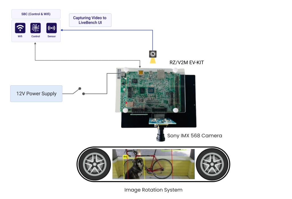
While LiveBench can accommodate a wide range of designs, there may be limitations for certain devices requiring highly specialized equipment. It’s best to consult with Tenxer Labs to ensure compatibility with your specific designs.

In addition to the above, there are complete systems like Drones etc can’t be deployed in the lab for now.

LiveBench is ideal for designs targeting a broad market with a high number of potential customers. “Custom-built” designs for one or two clients or those requiring complex protocol analysis may not be the best fit for this platform.

Tenxer Labs is responsible for maintaining the evaluation labs where the LiveBench platform is hosted. This includes ensuring the proper functioning of the equipment and maintaining a secure environment.